EMPA
EMPA
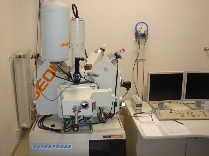
The JEOL JXA-8200 Superprobe in our institute is a high resolution SEM and a WD Electron Probe Microanalyzer (EPMA). The Electron gun consists of a tungsten cathode. Five wavelength dispersive X-ray spectrometers (WDS) the possibility of efficient and accurate analysis. The WDX spectrometers are able to analyse all elements Z > 3 with different crystals (LIF, PET, TAP) and LDE1, LDE2, LDEB for light elements (Be, B, C, N, O, F). In addition one can observed specimens with a visible-light microscope (reflected and transmitted light). This equipment allows to determine the chemical composition of different samples.
The high-speed large specimen stage (HSLSS XM-81010) belongs to the Electron Probe Microanalyzer can handle samples up to 9 x 9 x 2 cm (L x B x H) through the airlock, and can reposition a sample to less than 0.5um.
Please contact the Chair of Applied Mineralogy for further information.
The Jeol Superprobe with 5 Spectrometers and EDX system
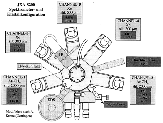
Configuration of Spectrometers and diffraction crystals of the Electron Probe Microanalyzer JXA-8200 (according to A. Kronz)
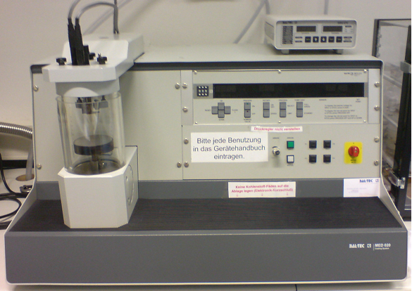
Sputtering- and Coating Device MED 020, Co. BAL-TEC
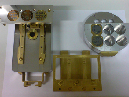
Specimen Stage (including standard materials) with specimen holder for thin- and thick sections
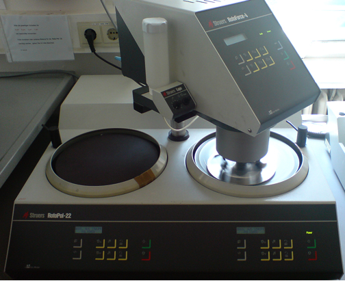
Grinding- and Polishing Device RotoPol-22 Co. STRUERS for thick and thin sections
The Electron Probe Microanalyzer JEOL JXA-8200 has the following specifications, parameters and capabilities:
- Five wavelength-dispersive spectrometers (WDS):
- Detectable element range: 4-Be to 92-U (all elements with Z > 3).
- Eight crystal types: TAP, PETJ, PETH, LDE1, LDE2, LDEB, LIF, and LIFH.
- Layered dispersive elements, gas-flow detectors allow light-element analyses.
- Secondary-electron (SE) and backscattered-electron (BSE) imaging:
- SE image resolution: 6 nanometers (at 30 kV accelerating voltage; 11 mm WD).
- BSE image modes: composition (sum) and topography (difference).
- Multi-element line analyses and area maps
- Matrix corrections using ZAF.
- High-speed large specimen stage (HSLSS XM-81010):
Maximum sample size: 100 x 100 x 50 mm (H).
Maximum analysable area: 90 x 90 mm.
- Accelerating voltage: 0.2 to 30 kV (0.1 kV steps).
- Electron probe current range: 10-12 to 10-5 A
- Electron probe current stability: ± 0.5 x 10⁻³/h; ± 3 x 10⁻³/12h
- Integrated visible-light microscopy: transmitted and reflected light